- 您现在的位置:买卖IC网 > Sheet目录3861 > PIC16C711-20/SO (Microchip Technology)IC MCU OTP 1KX14 A/D 18SOIC
140
7593L–AVR–09/12
AT90USB64/128
Bit 2:0 – CSn2:0: Clock Select
The three clock select bits select the clock source to be used by the Timer/Counter, see Figure
If external pin modes are used for the Timer/Countern, transitions on the Tn pin will clock the
counter even if the pin is configured as an output. This feature allows software control of the
counting.
15.10.5
TCCR1C – Timer/Counter1 Control Register C
15.10.6
TCCR3C – Timer/Counter3 Control Register C
Bit 7 – FOCnA: Force Output Compare for Channel A
Bit 6 – FOCnB: Force Output Compare for Channel B
Bit 5 – FOCnC: Force Output Compare for Channel C
The FOCnA/FOCnB/FOCnC bits are only active when the WGMn3:0 bits specifies a non-PWM
mode. When writing a logical one to the FOCnA/FOCnB/FOCnC bit, an immediate compare
match is forced on the waveform generation unit. The OCnA/OCnB/OCnC output is changed
according to its COMnx1:0 bits setting. Note that the FOCnA/FOCnB/FOCnC bits are imple-
mented as strobes. Therefore it is the value present in the COMnx1:0 bits that determine the
effect of the forced compare.
A FOCnA/FOCnB/FOCnC strobe will not generate any interrupt nor will it clear the timer in Clear
Timer on Compare Match (CTC) mode using OCRnA as TOP.
The FOCnA/FOCnB/FOCnB bits are always read as zero.
Bit 4:0 – Reserved bits
These bits are reserved for future use. For ensuring compatibility with future devices, these bits
must be written to zero when TCCRnC is written.
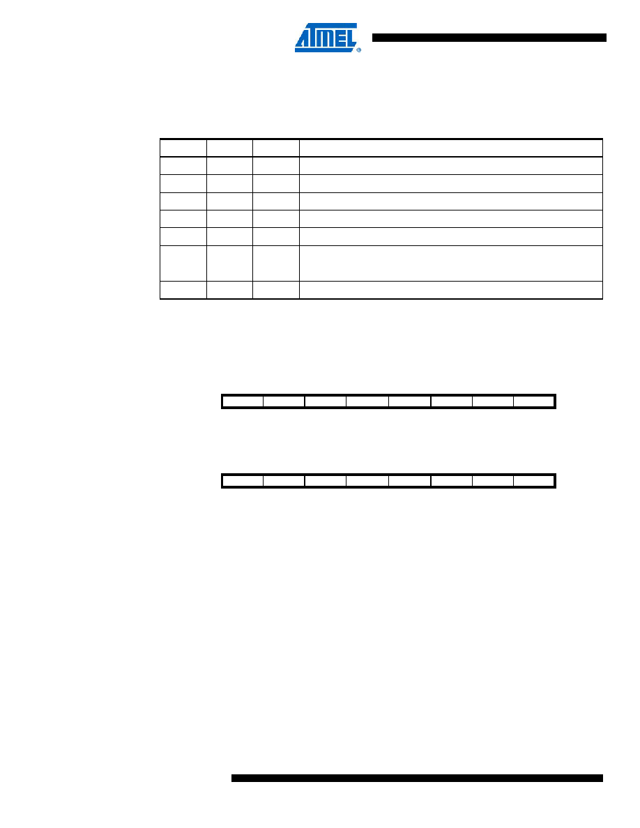
Table 15-5.
Clock Select bit description.
CSn2
CSn1
CSn0
Description
0
No clock source. (Timer/Counter stopped)
00
1
clk
I/O/1 (no prescaling
01
0
clkI/O/8 (from prescaler)
01
1
clkI/O/64 (from prescaler)
10
0
clk
I/O/256 (from prescaler)
10
1
clkI/O/1024 (from prescaler)
1
0
External clock source on Tn pin. Clock on falling edge
1
External clock source on Tn pin. Clock on rising edge
Bit
7
6
5
4
3
210
FOC1A
FOC1B
FOC1C
–
TCCR1C
Read/write
W
R
RRR
Initial value
0
Bit
7
6
5
4
3
210
FOC3A
FOC3B
FOC3C
–
TCCR3C
Read/write
W
R
RRR
Initial value
0
发布紧急采购,3分钟左右您将得到回复。
相关PDF资料
PIC18F44J50-I/ML
IC PIC MCU FLASH 16K 2V 44-QFN
PIC18LF26J50-I/SS
IC PIC MCU FLASH 64K 2V 28-SSOP
SFW19R-2STE1
SFW19R-2STE1-FFC/FPC CONN
HFW30R-2STE1
HFW30R-2STE1-FFC/FPC CONN
PIC18LF44J50-I/ML
IC PIC MCU FLASH 16K 2V 44-QFN
AT90S1200-12PI
IC MCU 1K FLSH 12MHZ IT 20DIP
AT90S1200-12PC
IC MCU 1K FLSH 12MHZ 20DIP
PIC16LF87-I/SO
IC MCU FLASH 4KX14 EEPROM 18SOIC
相关代理商/技术参数
PIC16C711-20/SO
制造商:Microchip Technology Inc 功能描述:8BIT CMOS MCU SMD 16C711 SOIC18
PIC16C711-20/SS
功能描述:8位微控制器 -MCU 1.75KB 68 RAM 13 I/O 20MHz SSOP20 RoHS:否 制造商:Silicon Labs 核心:8051 处理器系列:C8051F39x 数据总线宽度:8 bit 最大时钟频率:50 MHz 程序存储器大小:16 KB 数据 RAM 大小:1 KB 片上 ADC:Yes 工作电源电压:1.8 V to 3.6 V 工作温度范围:- 40 C to + 105 C 封装 / 箱体:QFN-20 安装风格:SMD/SMT
PIC16C711-20E/P
功能描述:8位微控制器 -MCU 1.75KB 68 RAM 13 I/O 20MHz ExtTemp PDIP18 RoHS:否 制造商:Silicon Labs 核心:8051 处理器系列:C8051F39x 数据总线宽度:8 bit 最大时钟频率:50 MHz 程序存储器大小:16 KB 数据 RAM 大小:1 KB 片上 ADC:Yes 工作电源电压:1.8 V to 3.6 V 工作温度范围:- 40 C to + 105 C 封装 / 箱体:QFN-20 安装风格:SMD/SMT
PIC16C711-20E/SO
功能描述:8位微控制器 -MCU 1.75KB 68 RAM 13 I/O 20MHz ExtTemp SOIC18 RoHS:否 制造商:Silicon Labs 核心:8051 处理器系列:C8051F39x 数据总线宽度:8 bit 最大时钟频率:50 MHz 程序存储器大小:16 KB 数据 RAM 大小:1 KB 片上 ADC:Yes 工作电源电压:1.8 V to 3.6 V 工作温度范围:- 40 C to + 105 C 封装 / 箱体:QFN-20 安装风格:SMD/SMT
PIC16C711-20E/SS
功能描述:8位微控制器 -MCU 1.75KB 68 RAM 13 I/O 20MHz ExtTemp SSOP20 RoHS:否 制造商:Silicon Labs 核心:8051 处理器系列:C8051F39x 数据总线宽度:8 bit 最大时钟频率:50 MHz 程序存储器大小:16 KB 数据 RAM 大小:1 KB 片上 ADC:Yes 工作电源电压:1.8 V to 3.6 V 工作温度范围:- 40 C to + 105 C 封装 / 箱体:QFN-20 安装风格:SMD/SMT
PIC16C711-20I/P
功能描述:8位微控制器 -MCU 1.75KB 68 RAM 13 I/O 4MHz Ext Temp PDIP18 RoHS:否 制造商:Silicon Labs 核心:8051 处理器系列:C8051F39x 数据总线宽度:8 bit 最大时钟频率:50 MHz 程序存储器大小:16 KB 数据 RAM 大小:1 KB 片上 ADC:Yes 工作电源电压:1.8 V to 3.6 V 工作温度范围:- 40 C to + 105 C 封装 / 箱体:QFN-20 安装风格:SMD/SMT
PIC16C711-20I/P
制造商:Microchip Technology Inc 功能描述:IC 8BIT CMOS MCU 16C711 DIP18
PIC16C711-20I/P
制造商:Microchip Technology Inc 功能描述:Microcontroller IC Num of I/Os:13